
Juggernaut | ASML - A Long Time Coming (Full Write-Up)
A deep dive on the Dutch Photolithography giant "ASML" and its chokehold on the semiconductor industry.

Jug·ger·naut
noun
a huge, powerful, and overwhelming force or institution.
Juggernaut is a strong word, but when you have a single company with a chokehold on the entire manufacturing processes of humanity’s most important technology (semiconductors) then you get to use a word like juggernaut.
When that company grows its earnings at a 20% CAGR over 10 years, achieves 30% net margins, has a returns on equity of ~50%, and is currently trading at 26x TTM earnings…you better believe i’m gonna write about it.
ASML is a beast of a company. Its wildly important to the global economy, has wonderful economic characteristics, and has been trading for a surprisingly cheap price recently despite being a sort of “pick-and-shovel” on AI. Moreover, ASML is not among the large cap tech companies included in the overheated U.S index’s - i.e its not exposed to any potential passive-index “overpricing.”
I know this isn’t the first write-up on ASML, but i’d like to try my hand at explaining why this company is so appealing to me; as well as some features most investors overlook.
But to talk about ASML, we have to talk about semiconductors - a topic I always enjoy talking proselytizing about. I’ve explained some of this already in my write-up on the China/Taiwan situation, so prepare for a little repetition. And if you’re new to the Margin of Sanity, prepare for my signature-abuse of the word “brief.”
How Computers Work: A Brief Explanation
Ok, i’m really going to try this time to keep it brief, but if we don’t understand computers then we don’t understand chips. If we don’t understand chips then we can’t understand chip-making equipment. And ASML is a “chipmaking-equipment” company, so…yeah we’re gonna talk about how computers work.
Have you ever seen a movie where someone uses morse-code? For example, imagine someone flipping a light: “on, off, on, on, on, off, off, on, off, on off off off (ect)” and somehow this communicates a message via a pre-established code? Well, this is sort of how you can think about the most basic form of computing.
01010011 01110101 01100010 01110011 01100011 01110010 01101001 01100010 01100101
Look familiar? Yeah, don’t worry - we’re not here to learn binary code. But know this: in order for binary code to be anything other than theoretical, it must be represented electrically (like a light switch turning on/off). And so it is; in a type of circuit called a “transistor.”
Now, the transistor has existed for almost a century, and I don’t mean to prattle on about rudimentary electrical engineering, but the important thing about a transistor circuit is that it does two things…
it goes “ON” = 1
and “OFF” = 0
Is this clicking yet? Because whatever machine you are reading this on is currently producing billion or trillions (or more…probably more) of electric signals that are - in their simplest form - either an “on” or an “off”: either a 1 or a 0.
1’s and 0’s are our world. Our entertainment, medical history, dating profiles, Substack subscriptions (hint); literally everything that exists in electrical form is ultimately represented by 1’s or 0’s - and need gazillions of “transistor circuits” to exist.
The transistor circuit began as a series of wires and electrical components you could see and manipulate with your hands, but then evolved into small microscopic patterns on tiny silicone chips. Today they are nano-scopic.
For decades now, these circuits have contained no “tiny copper wires,” but instead exist on chips of silicone (perhaps you’ve heard of Silicon valley). Why silicone? Because silicone is neither conductive nor resistant to electrical charge. Instead it is semi-conductive because it only becomes conductive when it has a charge running through it. This gives one the ability to control whether their circuit is connected (on) or disconnected (off)…..1 or 0.
I’m off on a tangent here so lets bring it back to size. Nanometers. This is the size we’re talking about when we talk about modern transistor circuits - which we just call “semiconductors” today. For reference, your fingernail grows about a nanometer every second, and the smallest features on the smallest chips are about 2 nanometers. So yeah, that may give you some idea of how small these gajillions of little on/off switches have to be to fit in your phone and do…whatever you want…all the time.
These chips aren’t just in phones, computers, and data-centers; they’re in cars, airplanes, lightbulbs, electric grid monitoring systems, oil rigs, a million other things, and oh right…military equipment. As a matter of fact, the future of modern warfare depends on technological supremacy, and these chips are 100% critical to all of it.
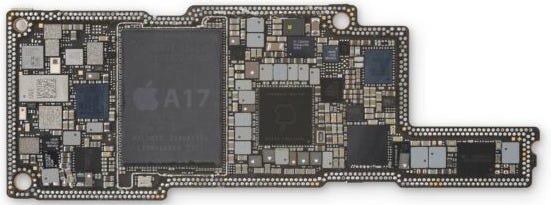
Above you’ll see the circuitry inside an Iphone 15 Pro. The black box in the center marked “A17” is the CPU chip (manufactured by TSMC). That chip contains 19 billion individual transistor circuits (on/off switches). When you’re using your phone, those 19 billion switches “flip” from on to off millions if not billions of times in a second.
If you’re thinking, “how in the world does one make something like that,” then you’re in the right place.
How In the World Does One Make Something Like That?
The world of chip manufacturing is currently dominated by TSMC (one of my largest/oldest positions). Intel, Samsung, Micron, and a few other companies also manufacture chips, but TSMC does it best. The basic process, however, is somewhat universal.
The overly-simple version is this: a circular, mirror-flat sheet of silicone (called a wafer), is coated with various chemicals - called “photoresist” - which resist light. A “lithography machine” then shines extremely small light waves through a sort of “stencil” to create a pattern on the photoresist film. That newly stenciled film is “developed” and another machine then “etches” that pattern onto the wafer. After the initial pattern is etched onto the silicone wafer, the chemicals are removed, and the sheet of silicone is sent back to a process called “deposition” where various materials are “deposited” onto the wafer, more photo-resist chemicals are added, and another stencil patterns that new layer.
And this process repeats again…and again…and again…and again…and AGAIN…
For months.
I’m seriously under-explaining the entire process because its so complicated, but if you want to get a real idea of all the steps that go into a making a microchip, here is a fantastic video which depicts the process.
When that wafer - which you can picture as a sort of microscopic “layer cake” or “apartment building” is complete - little pieces of it are broken off (or chipped off - yes thats where the term comes from), and you have your semiconductor chip.
If you look inside a chip fabrication plant (also called a “fab”), you’ll see a bunch of machines, each of which is responsible for one part of the process. Wafers are carried via automatic railways in the ceiling to each machine, and one machine in particular is responsible for shining that absurdly small and precise light pattern onto the wafer (again and again and again).
This is what is known as a “photolithography” machine, and it is often regarded as the most complex piece of equipment mankind has ever created (space-shuttle be damned). Without it, we could not make chips. Each machine is about the size of a double decker bus and can costs in the hundreds of millions of dollars. These monsters are so vital to the manufacturing process that repairs and maintenance are performed by a Formula-1 style pit-crew of engineers and technicians. However complicated and intricate you think this machine is, its 100x crazier, and there is one company on Earth that makes it:
ASML
Below is a video which explains/describes the role of ASML’s photolithography machines in the chipmaking process, and I highly recommend watching at least the first 5 minutes.
“Nanoscopic Micro-chip Photocopiers” is probably the best description i’ve heard for what ASML’s machines do.
This process of patterning - shining light through a patterned stencil (of sorts) - is as fundamental to chipmaking as any of the other steps in the process. Below is a breakdown of the various “stages” in the process, as well as guide to which companies supply equipment for said stage.
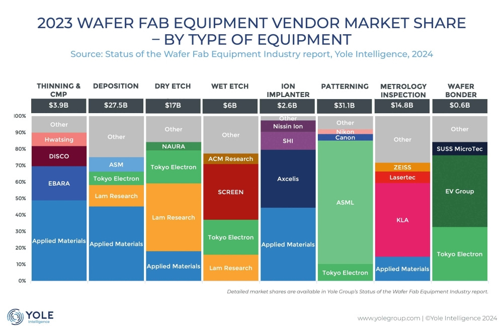
You’ll notice that the “Patterning” stage is dominated by a single company: ASML. Since Tokyo electron doesn’t make photolithography machines, but instead supplies more “supportive” equipment for ASML, it shouldn’t be counted as a competitor to ASML. When it comes to Canon and Nikon, these two companies only produce the older lithography machines (DUV). We will get to DUV lithography soon, but essentially these machines produce older “legacy-node” chips, and not the cutting-edge stuff that we often refer to when we discuss chip making. Still, the DUV market is rather huge, and we shouldn’t discount it. That said, within the DUV market, ASML still enjoys about an 85-90% market share. When it comes to cutting edge EUV lithography, ASML is the only game in town. We’ll break that all down soon.
Equipment manufacturing is usually the sort of business I would avoid, but ASML’s complete dominance makes it interesting to me. Competing with ASML is not as simple as building a new factory or poaching some talent. This Dutch company is decades old and has spent that time acquiring their own suppliers and entrenching themselves into an obscenely complicated world of engineering. No one else comes close, and to actually try to compete is a fools errand - extremely costly and unlikely to succeed. ASML itself is almost like a country, or a sort of engineering diaspora. “Moats” come in all shapes and sizes, and this one is particularly difficult to climb. As I said, ASML has a history of acquiring its suppliers (companies who produce highly specialized optical equipment). Decades of billions of dollars spent annually on acquisitions, R&D, and Capex mean that ASML’s moat gets deeper every year as their technology advances well beyond the capabilities of any other companies - and their market share ever-more out of reach for any potential “competitors.”
In short: “one does not simply start competing with ASML.”
And before you start thinking this is some “capital-intensive monster-conglomerate,” let the record show that ASML’s return on assets has remained above 10% going back to 2017, and currently sits at 20%. Return on equity is even higher (over 20% since 2019) and currently stands at 50%. And no, its not a leverage thing; ASML’s cash on hand is consistently greater or equal to it’s long term debt.
We’ll dive deeper into financials soon enough, but first lets talk about the business.
The Business
ASML reports two categories of revenue: “System Sales” and “Service and field option sales.”
System Sales
This is by far the largest driver of revenue with €21.7 billion in sales for 2024. “Systems Sales” is likely what most people think about when they discuss ASML. In short, when ASML sells one of those massive, bus-sized lithography machines, that’s a sale of a system (i.e: “systems sales”). Simple.
ASML has two main systems types that its sells: DUV (Deep Ultraviolet) and EUV (Extreme Ultraviolet).
As we know, ASML’s photolithography machine are “microchip photo copiers,” and the patterns they make are so small (nano-scopic) that normal “light waves” are way too big. Yes…normal light is soooo 1999. As a matter of fact, since the late 90’s, ASML’s machines exclusively employ use of “ultraviolet light” because it allows them to pattern ever-smaller transistor circuits onto the silicone wafers. The infamous “Moore’s Law” wouldn’t exist without ASML’s ability to produce ever-smaller patterns (and do so using smaller light waves).
The “old machines” are called “DUV” (deep ultra-violet), but since 2013 ASML has been shipping extreme Ultraviolet lithography machines. And today, the “hot new thing” is called “High-NA EUV” (NA = numerical aperture). I’ll discuss each one in a moment, but just know that there are DUV machines and EUV/High-NA EUV machines. And yes, ASML still does a ton of DUV business as it turns out plenty of chips don’t really require “the latest and greatest.” Regardless, every time ASML sells one of these monstrosities, it gets booked as “Systems Sales.”
Beyond DUV and EUV (which includes High-NA EUV), there is also HMI systems.
HMI = Hermes Microvision, Inc., a Taiwanese company ASML bought in 2016. They make e-beam (electron beam) inspection and metrology tools. These aren’t lithography machines - they’re like super-microscopes that fabs use to check if the patterns printed on the wafer are correct. The HMI segment is part of what ASML calls “holistic lithography.” Naturally, if the chip has even one imperfection the whole thing is useless, so “inspection” is very important. Imagine if you bought a new iphone and it was broken right out of the box. No good.
The Systems Sales segment accounted for 77% of total 2024 revenue and enjoyed a 52% gross margin for the year.
Service and Field Option Sales
The remaining 33% of revenue comes from what amounts to a sort of subscription-type “services” segment. When ASML sells a machine, the customer still pays ASML to help “service” and maintain the equipment in the field. Each machine is very expensive (€100-€500m each) and its also 100% critical to chip-fab operations. Simply put: when it goes down, it costs big bucks. For every hour one of ASML’s machines is out of service can cost a chip fab ~€50k-€100k (every hour). When you rely on a machine like that, you don’t let it fall into disrepair; enter ASML’s services arm. The most complicated machine ever made requires expert service technicians, and these people come from ASML directly (this is a car you have to take directly to the dealership).
Beyond maintenance and repair, ASML also offers other “upgrades” for their machines, and these “Field option sales” also get bundled into this revenue category. Gross margin on this segment was 48% in 2024. I’ll only note that i’ve heard others refer to this as the “high margin” segment, but it should be noted that it is not. Just because its a service, doesn’t mean its super high margin.
That said, ongoing revenue from an installed base of equipment (think Pool Corp’s chlorine sales being driven by new-pool builds) is a solid setup for any business.
So, there it is. Systems and Services. Lets dive deeper into systems
Systems (a deeper look)
ASML’s EUV and “High NA-EUV” machines make a lot of headlines, but a look at the numbers tells us that demand for DUV is alive and well - making up more than half of total systems sales. Below you’ll see revenue figures for all three systems segments splayed out across 8 years, and the story is clear. DUV has steadily grown, augmented by adoption of EUV technology. HMI has also grown over the years, but still represents a relatively small (€646m) portion of 2024 revenue.
2024 is the first year ASML sold any High-NA EUV machines (a.k.a “EXE”) and this accounted for a mere €465m of the ~€8.3 billion in EUV revenue in 2024. The growth story appears to me to be two-fold. The first part is selling older “DUV” machines to fabs that produce legacy nodes (think automotive, consumer electronics, memory chips, and a million other things), and the second is the growth in adoption of EUV to make more advanced chips (think GPUs and CPU’s for AI data-centers, smartphones, and computers).
While ASML holds a 100% market-share in EUV equipment, the DUV market is where some competition does exist (Nikkon/Cannon). As mentioned earlier, ASML still holds close to a 90% market share in DUV, but lets just understand the moat on DUV a bit better.
While other companies can produce DUV machines, ASML’s are far superior (faster and more precise). Perhaps more importantly, they’re also the industry standard. Because ASML’s DUV machines are already in almost all fabs on Earth, when these engineers set out to design the fab, they’re not planning for Nikon. Semiconductor Fabs are basically small cities that cost tens of billions of dollars to build. Design is incredibly complex and critical, so why the hell would you design your $50 billion fab to run on Cannon’s cruddy lithography equipment. As it stands, the only people buying Cannon and Nikon gear are cruddy fabs looking to produce very old nodes for cheap. As it stands, those machines are fine if you’re producing >90nm, but for reference, to build a new iPhone (A17 Pro chip, 2023–2024) you need a 3nm chip (made by TSMC using EUV machines).
Even the least compute-intensive parts of an automobile require sub-90nm chips, but sure, the school calculators we used as kids could have been made by Nikon’s lithography equipment.
So lets start by digging into DUV. Below you’ll see the four types of DUV lithography machines ASML sells going back to 2016.
***NOTE: Wavelength and node sized are not the same thing. ArF Immersion, for example, uses a light with a 193nm wavelength, but can produce chips as small as 7nm node.****
ok, now lets get into it
ArF Immersion (ArFi, 193 nm wavelength)
ArF immersion is the most advanced type of DUV lithography, and accounts for most of ASML’s DUV sales. The “193 nm” refers to the wavelength of light used - but through clever optics and a layer of ultra-pure water between the lens and the wafer, engineers can effectively push resolution well below what 193 nm would normally allow. This “immersion trick” bends the light more tightly and increases the “numerical aperture”, which lets fabs etch much smaller patterns. ArFi tools are used for process nodes down to ~28 nm and smaller, and with multiple exposures and patterning steps, fabs even pushed ArFi into 7 nm and 5 nm production before EUV arrived.
Today, ArFi is still widely used in DRAM and NAND memory production, as well as in many layers of leading-edge logic chips, even those otherwise built with EUV. It’s ASML’s most important and highest-value DUV product line. No other company makes an equivalent machine, and China - try as they might - has seemingly also failed to advance to this level.
Another fun fact is that China used to be able to buy these ArF Immersion systems from ASML until the Dutch Government (under pressure from the U.S) forced ASML to stop selling ArF Immersion chips to China in 2023. By 2024, the deal was finalized, but SMIC (China’s primary chip-maker) had already stocked up big time on ArF Immersion systems. So if you’re wondering what lithography machines manufactured the chips in Huawei phones, its these.
Cost: €70–120M per tool depending on config and generation.
ArF Dry (193 nm dry)
ArF dry scanners also use 193 nm light but without the immersion step. Without water to boost resolution, these machines top out at larger geometries and are typically used in the 65 nm to 130 nm range. They’re less complex and cheaper than immersion tools, which makes them attractive for mature logic and analog fabs that don’t need cutting-edge patterning.
You’ll find chips made with ArF dry tools in things like midrange microcontrollers, mixed-signal chips, and older networking or communications parts. They’re not glamorous, but they’re still essential for the long tail of semiconductor demand.
These machines are also made by Nikon (not Cannon), and China’s SMEE (Shanghai Micro Electronics Equipment) claims to have “prototypes.” Regardless, ASML still makes the best ArF Dry systems.
Cost: €30–50M
KrF (248 nm)
KrF lithography uses a longer wavelength, 248 nm, which makes it suitable for 90 nm to 250 nm process nodes. These machines are the backbone of many mature-node fabs, and make up the second largest category of ASML’s DUV systems sales. They’re heavily used to make display driver chips (for phones, TVs, laptops), power management ICs, CMOS image sensors, MEMS (like accelerometers and microphones), and automotive microcontrollers. Because autos and consumer devices need such massive volumes of these kinds of chips - and because those chips don’t need to be as tiny as an iPhone processor - KrF systems are still in demand. Even though they’re “older” tech, they underpin many industries that have huge, stable markets.
China’s SMIC uses KrF systems to produce the chips in all those BYD cars you hear about (as well as a lot of consumer devices).
Cost: €15–25M
i-line (365 nm)
This is the most “blunt” and….lets say “old school” type of ASML machine. I-line tools use 365 nm light, which is even longer wavelength and much less precise, but perfect for very mature nodes above ~250 nm and even into the micron range. These machines are used for chips where performance isn’t about cramming billions of transistors into a square centimeter, but about reliability, robustness, and cost. Typical applications include power devices (for EV inverters or appliances), MEMS, LEDs, analog ICs, and cheap microcontrollers in things like calculators, thermostats, or washing machines. i-line is the oldest lithography still sold by ASML, but because these applications keep growing, especially in automotive and industrial power, the business is steady.
Cost: €5–10M
Now that we’re familiar with the four types of DUV systems ASML produces, we can take a look at the below chart to get an idea of the exact makeup of ASML’s DUV growth over time.
ArF Immersion is the clear powerhouse here, making up a larger share of DUV revenue than the remaining three systems combined. The massive spike in ArFi from 2022 to 2023 was driven by a chipmaking bottleneck combined with a surge in Chinese fabs trying to get ahead of regulations.
Below you can see ASML’s total revenue breakdown by region, and the Chinese surge in 2023 is rather evident:
The method of data-collection here differs from the way ASML books their actual revenue, so the YoY “decline” from 2023 to 2024 is not a reflection of ASML’s actual revenue for those two years (which actually show a modest increase YoY). Still, the breakdown should give you a comprehensive picture of who’s buying the equipment.
No surprise that Taiwan (TSMC), Korea (Samsung), U.S.A (Intel), and China (SMIC) are the top buyers, with Europe and Israel together making up a large portion of sales.
As TSMC expands operations to the U.S, Japan, and Europe, we should see a boost the revenue for those regions, despite TSMC being a Taiwanese firm.
Another KPI ASML tracks on their 10k is the “end use” for systems sales; logic vs memory. Once again, these numbers won’t align perfectly with those of the income statement, but its useful nonetheless in building a picture of the business. Below this chart i’ll post a table which will help describe what we mean by “logic” and “memory.”
Generally speaking, “logic” is for thinking and “memory” for remembering. Your computer uses both logic and memory in order to function. Examples of logic chips are CPUs, GPUs, AI accelerators, smartphone processors, microcontrollers in cars or appliances, and the little chips that manage Wi-Fi or Bluetooth. But what good is a computer without a memory? And so memory chips are the parts that store information so the logic can use it later. That includes fast working memory like DRAM and HBM, long-term storage like NAND flash and SSDs, and tiny SRAM blocks inside processors. When you train an AI model or run an app on your phone, the logic chip does the work, while the memory holds the data it needs - and ASML sells scanners to make both kinds, but they’re counted separately in its “logic” and “memory” revenue lines. For a fuller rundown of logic vs memory chips, see the table below.
While we’re still talking systems, let talk about throughput.
People often fixate on the size of the nodes (Moore’s Law) and ASML’s incredible progress over the years in building ever-smaller chips. It should be stated plainly that the size cannot and will not continue to shrink at the rate it has been - hence claims that “Moores law is dead.” And in many senses that is true, but “size isn’t everything” - as they say - and we should try and understand a bit more about what makes a lithography machine “good” besides its ability to produce nanoscopic circuits.
What Makes a Photolithography Machines “Good”
Like anything else in the world, it all depends on what you’re trying to do. If you want to build cutting edge semiconductor chips to try and create artificial general intelligence, you’re going to be purchasing a different machine than someone who wants to manufacture millions of cheap bluetooth earbuds. But there are a few qualities we can talk about when it comes to lithography machines.
Size
Ok, so size does matter of course, but in 2025 we’re damn close to the physical limits of how small a transistor can be. If you had asked me years ago, “how small do you think a transistor can be before basic particle physics renders it useless?” I would have given you a number that is about 1000x the size of what we ASML’s High-NA EUV machines produce today. So…yeah, don’t expect the chips of the future to be that much smaller than the ones we produce today. That said, size only matters on the cutting edge. As we’ve seen, most of the lithography systems that are sold each year are not producing cutting edge chips. The fact that ASML still dominates in ArFi and even other, more “archaic” lithography systems, tells me something else is going on.
Throughput
See, being on the cutting edge is wonderful, but legacy chip making is all about being a “low cost producer.” Just like any other commodity, the cheaper you make it, the better your margins. So with chip manufacturing, one of the ways to produce more for less is simply to produce chips faster than your competitors. In lithography systems, the bottleneck of speed is described as “throughput.” "In other words, how many wafers can you “put” through your lithography machine in an hour.
See, everyone loves to talk about size, but speed is one of the keys to a good piece of chipmaking equipment. Over time, ASML has improved the throughput of all of their systems. For example, when ArFi Technology was introduced back in 2003, the model at the time could produce ~65nm chips at a rate of ~120 wafers per hour, and today its producing sub 10nm at ~300 wafers per hour.
Accuracy
If you recall, wafers are built layer by layer by layer (like a nanoscopic 3D printed apartment building). Sticking with that metaphor, the accuracy of each layer really matters. When we’re talking about a massive 100-story building, “small” inaccuracies add up and inevitably result in a building that doesn’t stand the test of time. We need to be accurate to the millimeter when building each layer, or else the whole thing will fall down. Now shrink that apartment building by about a gajillion zillion percent and you have your wafer.
With semiconductor manufacturing, accuracy isn’t about millimeters, or even microns, its measured in those unbelievably small nanometers. So, essentially, the more accurate your lithography machine is, the better your “yields” will be (more functional chips per wafer). Of course, you can’t get much better than a 100% yield (today’s lithography systems are basically 99.9% accurate), but this is a very difficult metric to maintain as systems have gotten even smaller and aim to get even faster.
ASML’s “holistic approach to lithography” is part of what enables this level of accuracy. By involving themselves in more parts of the patterning process, ASML can squeeze better performance out of their core systems, and simultaneously upsell customers on “add-ons” and “upgrades” that no one else can offer. If we’re talking about “layer cakes,” then ASML isn’t just selling the oven, its selling the baking sheets, thermometers, and oven timers. (not a perfect metaphor, but you get the idea).
“Architectural Flexibly”
I’m sort of making that phrase up, but essentially i’m talking about wafer/chip/transistor design complexity. You know NVIDIA? Of course you do. Do you know what they do? They design chips and they need someone who can build these designs that get ever-more clever and complex with time. There is a reason i’m up 300% on my TSMC stock, and its because that company can produce those complex and cutting edge designs quickly, at high volume, and at a lower cost (thanks to higher yields). And TSMC needs ASML’s machines to do this. The fancy new “High NA EUV” machines aren’t necessarily about “smaller,” instead they’re about “more detailed and more complex.” So as we’ve reached the end of Moore’s Law, we can still make things more complicated, and for that we need the precision ASML’s latest machines.
So there it is! Its not just a game of size. Its a game of who can make unbelievably small things that are incredibly complex with unbelievable consistency. Oh right, and who can do all of that the fastest.
There’s one more element that makes up ASML’s systems moat, and it conveniently leads me to the other part of their business. “Services and upgrades” isn’t just another revenue stream for ASML, its also a huge part of their moat. When you purchase an older ArFi system from ASML, you not only get support and maintenance, but you also know you can upgrade it over time as the need arrises. TSMC, for example, hasn’t really been buying the High-NA EUV machines yet, as they’ve been able to upgrade and improve on their existing EUV systems. “The bears” often site this as a weakness, but I believe that to be a misguided conclusion.
Net Service and Field Option Sales: A Love Story
Every tool ASML ships is expected to run almost nonstop for 15–20 years. Fabs don’t just need the hardware; they need someone to keep it perfectly tuned, feed it spare parts, and teach it new tricks as technology moves forward. That’s where “Installed Base Management” - the company’s service and field-options segment - comes in. It’s the Gillette razor blade to ASML’s “Mach 5” razor, and it’s grown into a big slice of revenue.
“Field options” is ASML-speak for upgrades: new light sources, faster wafer stages, or smarter software that can squeeze out a few more wafers per hour or tighten overlay accuracy. Service contracts cover preventative maintenance, calibration, and emergency repairs. Together they create a recurring, high-margin stream that rises with every scanner sold. In some years, this installed-base business has grown faster than new system sales, because the number of machines in the field keeps climbing even when the capital-spending cycle pauses.
If you want to understand why ASML’s earnings don’t collapse every time chipmakers slow their capex, this is the answer. Service and field options turn the one-time sale of a scanner into a long-term annuity - steady cash that helps smooth out the bumps in the notoriously cyclical semiconductor industry.
People often site TSMC’s lack of urgency in purchasing the new High-NA EUV machines as evidence that fabs can just upgrade their old machines….but ASML is the one offering that to them, so in the end, ASML is getting paid either way.
People often think about ASML lithography equipment as if its a new Iphone that isn’t “cool enough” to warrant a new purchase, but thats such an oversimplifcation that its basically flat out untrue. ASML works together with chip-makers to better anticipate their needs down the road, just as TSMC works with Apple and NVDIA to understand their needs. This isn’t a “fuck you, pay me” type of industry, its one that relies on constant communication and collaboration across all verticals.
When fabs chose to upgrade existing equipment instead of purchasing the latest and greatest, they are actually just maximizing ASML’s total profits. To use the Iphone metaphor, imagine if instead of buying a new Iphone, you just paid to have yours refurbished, bought new airpods, a new charger, and a new case. And then when the need for a better CPU came around, you actually bought a new Iphone, and continued to use the old one for texts and emails. Now you’ve paid to upgrade, paid to maintain, and eventually made a new purchase when the need arose - plus you now have “apple care” on two devices.
Investors often make assumptions about ASML’s business that lead them down the wrong roads. They think the “moat” is simply that no one else can make an EUV machine, but lets not forget that ASML also has 100% market share on ArFi DUV machines - a larger portion of revenue than EUV. Why? Because ASML makes the best, and their tech is integrated into the ever-more-complex chipmaking process.
Service and maintenance contracts aren’t “optional,” they’re completely necessary. And ASML also doesn’t squeeze their customers, they work with them because they understand that the more money TSMC makes, the more fabs they’ll build, and the more they’ll end up spending in the long run.
As you might imagine, ASML’s service revenue grows along with its installed base.
So what does all this add up to at the end of the day? I think its time to break down the financials and see what we’re really buying with ASML.
Financials
We’ll start with the basics on the income statement, and i’ll try and throw in some more “creative” charts as we go.
First we can just take a look at the overall revenue by segment:
If you’re curious about gross margins for the Systems vs Services segments over time, take a look below:
I’ve often heard people reference the “high margin services” business for ASML, and I think the above chart shows that to be a bit of a myth. While, yes, service businesses usually do enjoy a higher margin, we just don’t see that evident in the numbers for ASML. That doesn’t mean its “low margin” by any means, but I think its a bit of misinformation that we should be weary of.
For any technology and innovation focused company, R&D spend is usually the most costly operating expense, and so I’ve included two charts that put ASML’s R&D in context with its gross profit:
Sure, its not Visa, but at ASML’s large scale, R&D spend seems rather “under control.” One of the advantages of being so far out ahead of any competition is that you don’t have to open the spending faucets just to stay in business. I will say that similar companies (Applied Materials and Lam Research), spend a few percentage points less than ASML on R&D relative to Gross Profit. This is perhaps a sign that ASML’s “monopoly” status doesn’t translate so well into the numbers. A good example of “not all moats are equal.”
Of course, this all translates into ever-growing net-income
And we can take a look at some pretty healthy margins below:
For an equipment maker these are solid margins, but they’re not so so spectacular compared to other chip-making equipment companies. Compared to Lam Research and Applied Materials, ASML’s net-margin is only a few percentage points ahead:
The 5 year average net margin for the three equipment makers are as follows:
ASML: 27.77%
Applied Materials: 24.83%
Lam Research: 25.49%
Once again, we don’t see the monopoly status of ASML taking noticeable shape in the numbers. That said, 27.77% net margin is a very solid result for a business like equipment manufacturing.
Moving on to the balance sheet:
A few quick health checks:
All I can really say is that ASML has a “sleep well at night” type of balance sheet. Considering they’re sustainably cash-generative (they don’t ever loose money), having this sort of net-cash positive/neutral position serves to give management some flexibility and security when things get uncertain. You’ll see the cash balance for 2024 skyrocket as ASML’s leadership buckled up for geopolitical uncertainty in the incoming U.S administration. Just remember that for when we start looking at Capex/capital returns.
On to the cash-flow statement.
Generally speaking, for a business like this the criticism is repeated use of the word “capital intensive.” So lets look at Capex, first, relative to the operating cash flow (all the cash generated by usual business activity).
Does that look like a company that over-spends on capex? Lets look at it on a percentage basis:
The operating cash-flow itself may be lumpy, but the above chart shows an average of ~20% of Op-cash being eaten by Capex. Totally reasonable for any company, let alone one that produced mankinds most complicated machine.
All of this adds up to high Returns on equity and assets, especially considering “assets” consist of so much cash, and “equity” doesn’t involve excess leverage.
Finally, lets just look at what is being spent vs what is being returned - while bearing in mind that 2024 involved that massive uptick in “cash on hand.”
Yes you’re seeing that right, in 2021 management spent almost 10 times the capex spend on buybacks. This is a company that returns cash to shareholders, but it doesn’t do so at the risk of its core business - hence the notable lack of buybacks in 2024 (when the stock was 30% more expensive than it is today and the geopolitical landscape became very uncertain for ASML).
Looking Forward (thoughts)
ASML’s price has come down a bit from its highs, and this is due almost entirely to managements cautious guidance (rather than disappointing financial results). Still, ASML’s management is very bullish on the future. They may say they’re being cautious, but they’re simultaneously building out more EUV manufacturing capacity as they expect demand to rise through 2030. While initially soft sales of High-NA EUV equipment are often cited as “proof of weak demand,” management doesn’t expect that to continue. If we want to look into the future of EUV, we can simply look at the evolution of ASML’s DUV business which is still growing despite the rollout of EUV fifteen years ago. As time goes on, ASML’s field upgrades and holistic approach to lithography means that existing equipment improves. These improvements come in many more forms than just “size of the chips.” ASML offers customers better throughput, accuracy, consistency, and scalability.
I think of my recent trip to North Africa where i’d guess almost none of the very old and low-end vehicles had any chips at all in them, let alone one made by an ASML machines. As time goes on and more of the world is lifted into the middle class, better transportation will demand better compute. That better compute will likely be patterned with ever-more DUV machines. At the same moment, developed nations are building out advanced HPC enabled data centers as fast as possible. These will be filled with chips made using EUV.
Its a mistake to think of the future only in terms of demand for the cutting edge, since ASML still dominates in the more sought-after DUV market. The existence of High-NA is proof that ASML is still innovating and improving for the future, and lack of demand is a symptom of being ahead…not behind.
Still, we should temper our excitement for ASML’s monopoly status. This is not a company that appears to be squeezing maximum dollars out of their business. They understand that overfishing would cause a semiconductor eco-system breakdown, and so their monopoly status is very much dormant. Yes, they aren’t fighting tooth and nail to win contracts, nor are they foregoing shareholder returns for pipe-dream technology, but don’t expect ASML to milk their structural advantages too much.
This is a strong company which - much like TSMC - is a pick and shovel on all technological improvement to civilization. If India were to chart a similar course to China, we could soon see an Indian chip-maker rise and begin buying ASML equipment to serve the needs of their 1.4 billion people.
Currently, AI seems to be the only story, but the numbers clearly show that ASML’s business is about a hell of a lot more than NVDIA chips.
As I wrote this, ASML’s stock rose from ~$720/share to $800/share (a very frustrating thing to observe). I need to meditate a bit on if that really matters to me. What I love is the lack of exposure to the glut in the S&P 500. I’m really starting to believe that the tide is rising too high in U.S equities, and ASML’s lack of inclusion in any U.S index means that it may actually not be too exposed to such overpricing.
Currently, ASML’s TTM P/E is still under 30 - historically this does not appear to be too “hot.” So I like it.
If I had to buy ASML today and close my eyes for 10 years I wouldn’t cry about it. Its a powerful company currently trading at a fair price due to what I believe to be inherently short term concerns. Its not a screaming deal at $800, but its fair. I’ll be keeping an eye out for any dips on ASML, and perhaps I’ll end up “missing the boat.”
Talk to ya later
-MoS
Disclaimer: Not investment advice. This publication is for education and entertainment only. Nothing here is an offer, solicitation, or recommendation to buy or sell any security. I may own (or short) securities mentioned and may change positions at any time without notice. Investing involves risk, including loss of principal. Do your own research and consider speaking with a licensed adviser who knows your situatio
Quite brief indeed. I did learn something about the older machines, despite being a shareholder alteady :) Thanks
This was so incredibly helpful. Thank you for taking the time to research and write